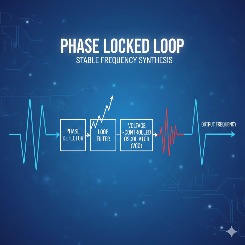
Phase Locked Loops
Engineering Academy
Learn Without Limits: Free Engineering Courses
FREE
1 already enrolled!
Advanced course for professionals

Anytime Learning

Learn from Industry Expert

Career Option Guideline
Phase Locked Loops
Why enroll
Opportunities that awaits you!

Earn a course completion certificate
Add this credential to your LinkedIn profile, resume, or CV. Share it on social media and in your performance review
Course content
The course is readily available, allowing learners to start and complete it at their own pace.
Phase Locked Loops
65 Lectures
1688 min
Course Introduction and Motivation Part I

Preview
39 min
Course Introduction and Motivation Part II
23 min
Basic Operation of a Phase Locked Loop
25 min
Simple Implementation of a Phase Locked Loop
16 min
Input Output Characteristics of Basic PLL Blocks
27 min
Time Domain Analysis of a Simple PLL
21 min
Time Domain Versus Small Signal Analysis of a Simple PLL
21 min
Type and Order of PLL
9 min
Small Signal Analysis of Type-I/II/III PLLs for Phase Step, Frequency Step and Frequency Ramp
30 min
Frequency Acquisition Range for PLLs
26 min
Frequency Acquisition in Type-I PLLs
32 min
Frequency Acquisition Limits in Type-I PLLs
18 min
Frequency Acquisition in Type II PLLs
16 min
Frequency Acquisition Ranges in Type II PLLs with Ideal and Non Ideal Integrator
37 min
Frequency Domain Insight in Frequency Acquisition for Type II PLLs
14 min
Introduction to Clock Multipliers
12 min
Analog Phase Error Detectors: Part I
35 min
Analog Phase Error Detectors: Part II
25 min
Digital Phase Error Detectors: Part I
32 min
Digital Phase Error Detectors: Part II
19 min
Range Extension for Phase Error Detectors
9 min
Phase Frequency Detector
31 min
Digital Frequency Detector
16 min
Charge Pump PLL
23 min
Small Signal and Stability Analysis of Type II Order 2 Charge Pump PLL
21 min
Problems in Charge Pump PLL - Dead Zone in PFD
13 min
Problems in Charge Pump PLL - Reference Spur
23 min
Design Procedure for Type-II Order 3 Charge Pump PLL
15 min
Design Procedure for Charge Pump Clock Multiplier
18 min
Sources of Non-Linearities in CP-PLL: Part I
32 min
Sources of Non-Linearities in CP-PLL: Part II
19 min
Noise Analysis in CP-PLL: Part I
31 min
Noise Analysis in CP PLL: Part II
43 min
Noise Analysis in CP-PLL: Part III
40 min
Noise Simulations for CP-PLL Blocks
16 min
Introduction to Oscillators
49 min
Low-Swing Ring Oscillator: Part II
15 min
Large-Swing Ring Oscillator: Part I
39 min
Large-Swing Ring Oscillator: Part II
23 min
Large-Swing Ring Oscillator: Part III
33 min
Large-Swing Ring Oscillator: Part IV
10 min
Large-Swing Ring Oscillator: Part V
43 min
Supply Regulated VCO: Part I
24 min
Supply Regulated VCO: Part II
33 min
Supply Regulated VCO: Part III
28 min
Phase Noise in Ring Oscillators
33 min
Circuit level Design of PFD: Part I
20 min
Circuit level Design of PFD: Part II
18 min
Circuit level Design of PFD: Part III
12 min
Circuit level Design of Charge Pump: Part I
31 min
Circuit-level Design of Charge Pump: Part II
13 min
Circuit-level Design of Charge Pump: Part III
12 min
Circuit-level Design of Charge Pump: Part IV
51 min
Circuit-level Design of Charge Pump: Part V
8 min
Circuit-level Design of Charge Pump: Part VI
39 min
Circuit-level Design of Clock Frequency Divider
36 min
Techniques for Wide Frequency Range Clock Multiplier
39 min
Introduction to Digital PLL
35 min
Design of Time-to-Digital Converter
38 min
Small Signal Analysis of Digital PLL
34 min
Noise Analysis in Digital PLL
38 min
Analog/Digital Hybrid PLL: Part I
37 min
Analog/Digital Hybrid PLL: Part II
52 min
Course Summary
15 min
Phase Locked Loops
3 min